Voltage Control Boosts Sensor Node Efficiency
Contributed By DigiKey's European Editors
2016-08-24
Wireless sensor nodes provide the driving force for the growth of the Internet of Things (IoT). The two most important aspects of wireless sensor nodes are that they should react to changes in their local environment and be energy efficient enough to survive on a single battery charge for years – possibly the entire expected lifetime of the sensor. To make sure the sensors react only to important changes, increasingly sophisticated software will be downloaded into them. This, in turn, calls for efficient processors such as those based on the 32-bit ARM® Cortex®-M architecture or, for simpler sensors, improved versions of 8-bit cores such as the 8051.
System-level power consumption is determined by many variables above and beyond the power efficiency of the processor itself. To improve efficiency, low-energy MCUs employ a number of intelligent peripherals to control hardware on behalf of the core processor. These peripherals operate at different times and will have power demands that change on a millisecond-to-millisecond basis. They need flexible power architecture to support this.
The reason for the need to control power to individual parts of the system and even to peripherals integrated into the MCU itself is to support a low duty cycle. The duty cycle determines how long during its lifetime the MCU processor is awake and processing data and how long it is powered down and asleep. A low duty cycle is important because the processor within the system spends almost all of its time asleep in order to save energy.
The low duty cycle strategy has proved highly effective in the design of utility meters where the processor core may sleep for 99 percent of its overall life cycle. It wakes only to collect data from sensor inputs, normally at a scheduled time or respond to unscheduled interrupts. Intelligent peripherals support this by checking data from inputs without needing to wake the processor. Only if a threshold is surpassed does the peripheral trigger an interrupt that will cause the processor to handle the change in circumstances. This strategy ensures that only significant changes are processed. Those that imply very little has changed can be queued in memory and handled when the processor core has been woken up for other reasons.
For example, in metering applications, a register encoder records the flow of natural gas or water as a series of pulses. Without hardware support, the MCU’s processor must wake up and sample the state of an I/O pin to determine if the switch is open or closed. If it is a physical reed switch, additional processing is needed to de-bounce the switch and to manage pull-up resistors to check it is a valid pulse and to minimize the current drain through the closed switch.
An energy-optimized approach is to use a dedicated input capture timer that can operate autonomously while the device is in sleep mode. The switch closures can be accumulated in a hardware register requiring little software intervention. Features, such as switch de-bounce, pull-up resistor management and self-calibration, can be integrated directly in the hardware. With two timer inputs, quadrature decode functionality can be supported to determine flow direction. This provides the capability of back-flow detection as well as an anti-tamper provision, both of which are used to trigger interrupts that let the processor react and send a warning message. A dedicated low-power input capture timer can consume as little as 400 nA at 3.6 V even with a sampling rate as high as 500 Hz versus more than 1 µA if executed in software.
Another example is that of preparing a message for RF transmission. The data must be manipulated several times. A 20-byte message payload that needs to be transmitted from the meter to the collector will be stored temporarily in SRAM once it has been prepared by software. To ensure its integrity after reception at the destination, a cyclic redundancy check (CRC) is computed and appended on the end of the message. Then the entire message needs to be encoded using a scheme (such as Manchester, 3:6) to improve transmission reliability. That encoded message is passed through a serial interface to the radio transceiver.
A dedicated packet-processing engine (DPPE) can be used to perform the CRC, encoding and relay to the transceiver far more efficiently than in software, allowing the processor to sleep while it happens. Using a DPPE not only reduces the time needed to perform the functions, but it also reduces the current consumption during that time as flash memory, which tends to demand a lot of current, is not being accessed. Instead, all operations are on local memory. The net result can be up to a 90 percent power reduction during active mode.

Figure 1: Comparison of execution time and current consumption for software and DPPE of packet CRC and encoding tasks.
To provide designers with a number of ways to reduce lifetime energy consumption, MCUs designed for this type of application provide a number of sleep modes that progressively withdraw power from the various component cores, storing their state in non-volatile memory or dedicated low-leakage registers, until almost all of the device has been powered down. For example, a deep sleep allows all but core peripherals such as the real-time clock to power down, which also removes the need to power circuits such as phase-locked loops that drive the on-chip logic clocks.
Low-energy sleep modes greatly enhance battery lifetime in sensor-node applications, but it is possible to go further and reduce power consumption when the MCU is active. During periods of activity, the power consumption of any logic circuit is given by the formula CV²f where C is the total capacitance of the circuit paths within the device, V is the supply voltage and f is the operating frequency.
To maximize system-design flexibility, the process technologies used by MCUs support voltages up to 3.6 V. However, because of the energy-consumption advantages of operating at lower voltages, the circuits inside will use a supply that may be set to 1.8 V or even less. Because it is relatively simple to implement, most MCU vendors use a linear voltage regulator, typically based on a low drop-out (LDO) design, to convert the input voltage from the battery pack into the desired internal supply; but linear converters trade their simplicity for low efficiency.
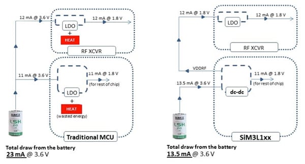
The problem is compounded by the need within a system for multiple LDOs to supply different peripherals external to the MCU, such as the RF transceiver, each of which may be supplied direct by the battery. The problem for this structure is that if, for example, the battery provides a voltage of 3.6 V to an RF transceiver that operates at 1.8 V internally, the conversion efficiency is just 50 percent. An RF transceiver that can take a voltage between 1.8 V and 3.6 V will improve its voltage-conversion efficiency as the input moves towards 1.8 V. This effect needs to be considered for each of the peripherals that are external to the MCU.

Figure 2: Comparison of energy efficiency for LDO- and DC/DC converter-based MCU designs.
The approach taken by Silicon Labs in MCUs such as the C8051F960 or the SiM3L1xx is to incorporate a switching DC/DC converter. The use of switched conversion results in higher efficiency. The technique uses pulse-width modulation (PWM) to feed packets of charge to the output circuitry, which smooths the packets using a combination of inductors and capacitors into a constant output voltage and current suitable for the load. An off-chip DC/DC converter can perform this function, but that adds to the component count of the system. The system may not be able to afford that when challenged in terms of size, which is often the case for sensor nodes.
In addition to reducing the MCU’s active mode current, the integrated high-efficiency DC/DC converter helps reduce the current demand of other parts of the system. By configuring the output voltage from the DC/DC converter to the lowest acceptable setting of the external peripherals that are controlled by the MCU and feeding them from the MCU’s voltage output line, the overall power consumption can be minimized. In the case of the external RF transceiver, the external voltage output can be set to 1.8 V and reduce its overall current demand.
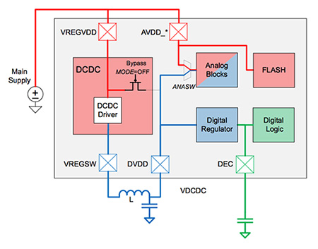
An integrated DC/DC converter provides greater opportunities in terms of circuit-level energy optimization where the designer can trade off voltage against performance to suit the target application. The Energy Management Unit on the EFM Pearl Gecko, for example, provides programmable control over the on-chip voltage regulators. This makes it possible to switch the regulator off when the battery voltage falls far enough to impact conversion efficiency and where it makes more sense to drive the MCU’s circuitry direct from the battery without an intermediate conversion. Another example of this in use is during sleep, where a simpler, low-current converter drives just the real-time clock to ensure that it will deliver the wakeup interrupts at appropriate times.

Figure 3: The internal voltage architecture of the EFM32 Pearl Gecko showing bypass lines.
Some circuits bypass the on-chip DC/DC converter to avoid the issue of performing a double conversion. For example, flash memory blocks normally incorporate a charge pump to provide the higher voltages needed during write operations to memory lines. Analog blocks may also be driven either by the direct battery supply or the DC/DC converter depending on application needs. For example, direct connection to the battery instead of a switching regulator will help reduce noise in the analog circuitry.
As a result, an MCU with integrated power conversion such as those in the Silicon Labs range provide the ability to tune energy consumption at the system level, delivering a far more efficient sensor node and longer battery lifetimes.

Disclaimer: The opinions, beliefs, and viewpoints expressed by the various authors and/or forum participants on this website do not necessarily reflect the opinions, beliefs, and viewpoints of DigiKey or official policies of DigiKey.


